Wednesday, April 29, 2020

Peak Force Kelvin Probe of Polyphase Polymers

In this example we look at polyphase polymers with PeakForce Kelvin probe microscopy. This sample consists of polystyrene (PS) with polydimethylsiloxane (PDMS) inclusions. These inclusions are soft, with an elastic modulus of 2.5-3.5 MPa, while the surround polystyrene is around 3 GPa.

This is a great sample for contrast in mechanical measurement techniques like PeakForce QNM, force volume, and so on. And it is a good representative of a soft sample that is well suited to PeakForce imaging where the peak normal force is known and controlled with minimal shear force. This allows for imaging under different peak normal forces, which can lead to different surface structures just due to deformation of the surface and interaction with subsurface structures.
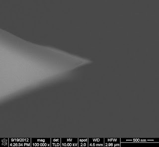
The top image is a height image taken with a peak normal force of 5 nN using a fairly stiff probe, a silicon SCM-PIT which has a spring constant of around 3 nN/nm. Deflection sensitivity was calibrated on sapphire, and the spring constant was estimated through thermal tuning to be around 2.1 nN/nm. This is stiff enough of a probe that the Sader method is more appropriate.

Since the SCM-PIT is coated with PtIr for EFM and KPFM, it was possible to do KPFM to image the surface potential. Initially this sample was chosen to calibrate the probe radius to  simultaneously do QNM and KPFM, to correlate both nanomechanical properties and surface potential properties of a different sample.

But-- why not KPFM on a soft biphasic polymer?

The bottom image is the raw PeakForce KPFM channel. The lift was 50 nm with a scan-rate of 0.1 Hz. A three hour image! What is immediately obvious is that the PDMS domains have a surface potential some 50-70 mV higher than the PS. There is also a potential "plateau" across the top left of the image, and athese little specs on some of the PS inclusions are clearly hitchhikers, contaminants, and they have a surface potential of 200-400 mV above the neighboring PS background.

Friday, April 24, 2020

KPFM and EFM of Exfoliated HOPG

In this demonstration, a piece of HOPG was grounded on the stage of the Bruker Icon using graphitic paint. An SCM-PIT probe was used to perform both PeakForce KPFM (Kelvin probe force microscopy) and EFM (electric force microscopy) on a region of the sample that presented broken edges of the exfoliated HOPG lamella.

The first image shows the height image taken in PeakForce mode. A normal force of about 10 nN was used, and even this is causing some disturbance of the graphitic lamella. Some of the sheets seem to come in multiple copies. This is actually not the result of a tip-artifact, as the effect goes away when switching to a lower peak force set-point, or when switching to tapping AFM in order to subsequently do EFM. The intermittent normal forces the sample sees in tapping AFM are much smaller than the 10 nN peak force used here. A larger peak force set-point was used only to help track the drastic topographic relief in this particular sample. This perturbation of the graphite lamella by 10 nN of peak normal force shows how flexible and loosely coupled they are.

The next image was taken in tapping AFM in lift mode to facilitate EFM imaging. EFM is an imaging mode that applies scanning interleave. There is one pass across the sample to image sample morphology, and then a second pass along the same trace-retrace. One can do anything one likes with the interleave pass. Take a second image with any change of parameters one likes from a different set of gains and set-point to a probe-sample bias. In this case the probe is lifted 100 nm above the surface of the sample and changes in probe amplitude and phase are detected. As in MFM (magnetic force microscopy) the amplitude change says something about the magnitude of an electric field gradient, and a phase change says something about its sign-- whether it is repulsive or attractive as seen by the probe.


The results were are quite curious. HOPG is quite a good conductor, and the sample was well grounded using graphitic paint. It is interesting that any EFM signal is seen whatsoever given that it is not biased. The signal is small. There is only about a 0.5 nm amplitude change across the whole image region, but it clearly correlates with the edges of the lamella. The edges are the source of a gradient.

Like MFM, EFM can be a bit difficult to interpret as one is probing an electric field gradient, and unless the geometry is of planar ferroelectric domains, or a planar fabricated device, it is often not clear what is causing these gradients: geometry, gradient in the potential creating the electric field, dielectric gradients. All that can be determined is that the magnitude of the EFM signal (i.e. the electric field gradient) is larger near the edges of the lamella, and trails off from there.

The EFM phase signal is, like the amplitude signal, very weak. About a half a degree of phase change over the whole image field. The signal is limited to the broken lamella edges and the rest of the lamellae are generally neutral in signal. This would seem to indicate a repulsive electric field gradient-- but it is harder to know what an electric field gradient says about the electric field itself. That is particularly the case in EFM where there are capacitive as well as charge effects that produce the EFM signal.

The last image is the KPFM which was done in PeakForce mode. This is actually measuring the surface potential in the interleave scan. What we see is an accumulation of potential on the broken edges of the lamella. Quite a small signal, a few 10's mV, but definitely consistent, repeatable, and correlating with the edges of the broken lamella. Given that this sample is conducting and well grounded with no applied potential to the probe or stage, this is surplus surface charge from the beaking of bonds?


Thursday, April 23, 2020

Multiple Scales of Artefacts

In this example, a tip roughness sample is imaged with a well worn Si probe. An image was taken in PeakForce mode with 5 nN of peak normal force. At 1 x 1 um the image is quite unremarkable. One might suspect a little probe wear based on the lack of resolution of some of the small grains. That could be a good thing if one were wishing to do some nanomechanical measurements or QNM mapping to get elastic moduli. But there is no obvious self-similarity to the objects, and no obvious companions. In the top left some quite small grains can be resolved on the larger grain. Structures well below 100 nm-- suggesting a good probe. Working out at 10 x 10 um would would anticipate good performance.

Except-- that is farthest from the truth. At the larger scan size there is nothing but self-similarity of the objects images, companions, preferred orientation-- all the signs that scream ARTEFACT.

The artefacts we see-- and don't see-- is a function of the 3D structure of the end of our probe, as well as the nature of the structures we are imaging. Their size and shape relative to the structures that define our probe. Here, a horribly damaged probe had a little tiny point on its end-- and that allowed quite good imaging at very small length scales. Above that, the blunt shape of the tip convoluted every feature into an array of heart- or bird-shaped artefacts.

Friday, August 10, 2018

Tin Nanospheres: A Tip Qualification Tool

Using a titanium sample for tip qualification is a standard procedure for certifying tip quality and for estimating the effective probe radius for nanomechanial measurements. This has been discussed in a previous post and while a reliable and quantitative method, it suffers the risk of damaging the probe in process of tip qualification as the titanium sample is quite hard. Another non-quantitative method is to use tin nanospheres on HOPG. Tin is quite soft and by controlling the substrate temperature nucleation can be controlled quite precisely. A sample with approximately 20 nm spheres is ideal for identifying a host of tip problems.  In truth they aren't "spheres" as they are only 8-10 nm tall and 20-ish nm in diameter

In this study several ScanAsyst Air SiN probes that "failed" were used to image this sample sample. PeakForce tapping was used with ScanAsyst, but any imaging mode would work. Because of the symmetric point-like nature of the objects, and because the radius of the Sn spheres (~ 20 nm) is close to the probe radius (~ 2 nm, but < 20 nm).

This allows one to effectively directly image the functional part of the probe. In the first two images one finds objects that look at least half-normal.

In the first image the spheres are all surrounded by something of a halo. The spheres are always in the left margin of this halo. In general, any image with self-similar features can be assumed to reflect imaging artifacts.

The second also reflects self-similar features. The objects all have a similar shape with a tail extending to the top left. What is interesting is that the density of objects is much higher as well. The objects all have multiple companions showing that the functional image surface is split into multiple parts.

While the first two images could be glossed as normal, the third and fourth images show radically damaged probes.

The last image shows a probe so broadened in radius that no objects are visible.


Friday, August 3, 2018

What Happens When A Probe Fails

There are many parameters that determine the performance of an AFM probe. These include the tapping frequency, spring constant, and probe radius. The spring constant is particularly important to control probe normal forces to mitigate shear forces or to provide the required normal force to deform surfaces in a specific range of modulus. Probe stiffness is also important in image quality when imaging soft materials.

The probe radius is the primary design parameter related to resolution. The process of tip qualification to measure the probe radius using a sample with sharp features has been discussed in a previous blog entry. An effective probe radius can be also be measured using controlled deformations while measuring the modulus of a material with known modulus. These methods of measuring probe radius are required for mechanical measurements as well as certifying image quality.

The degradation of the probe radius will impact image resolution as the surface features are convoluted with a larger than anticipated probe radius. A "sharp" probe might have a radius of 3-5 nm, so a blunting to 30-50 nm will result in the dramatic loss of image quality. Probes coated with conducting material, such as platinum or aluminum, will have additional artifacts in such modes as TUNA or conductive AFM in the current channels due to the loss of conducting contact area with the sample.

In this post visible apex AFM probes were imaged in a field emission SEM. This probe, the Bruker OTESPA, is called a visible apex probe because the functional part of the probe is at the very end of the cantilever, allowing one of locate objects of interest in the optical microscope of the AFM very easily. The probes were imaged with a 2 kV beam using the through lens detector and field immersion. The larger top image shows a good probe. Even at 2 kV parts of the probe appear to be "transparent" as SE1 secondary electrons are generated near the edges of the probe, while SE2 secondary electrons are generated from the thicker body of the probe.

It is common for probes to fail not only by being blunted or worn-- from their radius being drastically increased-- but from picking up objects. The smaller images show three examples of failed OTESPA probes. The probes showed lower resolution and in all cases either self-similar structures or features with companions. These SEM images show objects attached to the probe. In the second image a blunt object is stuck near the end of the probe, and the shape of this object where it contacts the surface would be convoluted with the sample features. In the third image a sharp object is attached just behind the probe. This can act as an companion probe that contacts features and probes companions or doubles to sample features. The last image shows deposition of material across much of the probe, and the attachment of a significantly large foreign object. An object of this size will not only degrade image quality by make the probe very unstable as it interacts with the surface.

The point of this post is to show that things really do go wrong with a probe when image quality degrades.

Wednesday, August 1, 2018

Power Spectral Density: Collagen D-bands (Part 2)

In a previous post, collagen D-bands were measured by sectioning an image. One sample of the D-band period was found to be 54 nm-- much less than the 67 nm found in TEM of stained histological specimens. While some variation is expected depending upon hydration, this is a significant discrepancy.

A fast Fourier transform (FFT) of the image is shown. A circular ring reflects the periodicity of the D-band spacing. This ring in the FFT is also broken reflecting the fiber orientation. Most of the intensity is between 11 and 1 o'clock as this reflects the orientation of the fibers with this D-band period. Another portion is around 2 o'clock representing the fibers at the top of the image that are diagonal in the image field. This is one useful application of the FFT: quantitating the orientation of structures in the image field.

The second image is 2D isotropic power spectral density. This reflects the power of image signal strength as a function of spatial frequency. The first maximum is at 64 nm and reflects the D-band spacing. As this includes spatial frequency information from the entire image, this is a much more robust method of estimating the D-band spacing than manually sectioning a couple D-band in an image.

Image Sectioning: Collagen D-bands (Part 1)

Images can be sectioned using the sectioning tool. In this case an image of human collagen was taken with PeakForce tapping. The image was flattened to remove large scale spatial relationships not related to the structure of individual collagen fibrils.

The D-bands arising from the staggering of tropocollagen structural units is clearly visualized on individual collagen fibrils. By drawing the sectioning tool across individual fibers, an effective digital cross section of the fiber along that line is produced. In this case the spacing between two specific bands is found to be 54 nm.  While the D-band period is a function of such environmental parameters as hydration, this is far less than the expected 67 nm seen in TEM of stained fibrils.

Application of the sectioning tool can be problematic as measurements are then biased according to the operator's selection of targets and placement of the dimensioning cursors. It is human nature of select features that are the least ambiguous and simplest to dimension by interacting with the image. As an example in this case I chose to section a long fiber in a cluster of long fibers. Removing operator bias would require a sampling methodology which covered more of the image field, including less "attractive" looking fibers, and statistically combining these measurements.

Human Collagen: PeakForce Tapping

The primary advantage of tapping AFM is that it is a non-contact AFM technique. While it "taps" on the sample surface, the tapping is intermittent and as such there is minimum shear force. This is ideal in imaging soft materials, including biological systems, as significant shear forces modify the sample surface while it is being imaged.

That tapping is generally done at the resonant frequency of the probe. A stiff silicon tapping probe has a resonant frequency on the order of 300 kHz, and so a tapping frequency just below resonance is selected for tapping AFM. Constraining the tapping causes the probe frequency to increase, and this will cause the probe frequency to move towards resonance not off resonance.

While this mode of imaging produces minimal shear force, one disadvantage is that it produces an indeterminate maximum normal force. While one can image in soft tapping mode by reducing the tapping amplitude, it is a non-trivial task to estimate the maximum peak normal force in tapping AFM. It is sometimes also desirable to know the maximum force exerted on a sample to quantitate sample deformation.

Bruker's PeakForce tapping combines the best of tapping and contact AFM imaging modes. What it does is perform complete force curves at 1-2 kHz at every image point. The force curve is triggered at the maximum applied normal force according to these force curves, and it is this "PeakForce" that is the set-point or parameter maintained constant during imaging. The second image, borrowed from Bruker, shows force curves as a function of time and position, and the PeakForce set-point is point C on both curves. A further innovation is ScanAsyst technology which dynamically and intelligently monitors and optimizes the scan rate, PeakForce set-point, gains, and Z-limit to produce the best image quality.

In this image human collagen from cadaver skin was imaged using a ScanAsyst Air probe in ScanAsyst mode. This image of a fairly soft biological specimen was imaged with little operator interaction beyond aligning the scanner and focusing on the sample. An additional advantage of the PeakForce tapping imaging mode is that force curves are available at every image point, and these can be used to perform nanomechanical measurements-- what is called PeakForce QNM.

Wednesday, March 19, 2014

Tapping AFM: Arabidopsis haliana Grana Membranes

Images of Arabidopsis thaliana grana membranes using tapping AFM. 

The Dimension 3000 AFM was used to image these membranes in air with stiff silicon probes (Olympus #OMCLAC160TS-W2, with 7 nm tip radius and 42 N/m spring constant). Arabidopsis thaliana grana membranes were isolated through treatment with 2% digitonin showing semi-crystalline array formation of photo-system II complex proteins due to changes in growth light intensity. Protrusions are the water splitting complex of photo-system II in photosynthetic membranes. Scale bar is 375 nm. 
 
Thanks to Stefanie Tietz and Dr. Helmutt Kirchoff, Washington State University Molecular Plant Sciences, as well as Dr. Steve Lenhert, FSU Department of Biology.

Monday, March 17, 2014

Lipid Grating

This image shows a dipalmitoyl phosphatidylcholine (DPPC) multilayer grating fabricated by lipid multilayer stamping. The image was taken in air using tapping mode, and is a good example of soft materials imaged in air using AFM techniques.

O. A. Nafday, T. W. Lowry, S. Lenhert, Multifunctional lipid multilayer stamping, Small 8, 1021-1028 (2012).

Sunday, August 12, 2012

Bruker Icon at CMMP

On 8 August 2012, the new Bruker Icon scanning probe microscope was installed at CMMP.  The Bruker Icon has ScanAsyst technology which allows for very high quality images to be made using the PeakForce scanning mode. It includes PeakForce QNM for performing nano-mechanical measurements, including the image of surface modulus, adhesion and dissipation.

To my knowledge this is the first Bruker Icon in the FL SUS. It was purchased through an EIEG grant through the FSU Office of Research with additional financial support from Dr. Steve Lenhert, (PI, FSU Biology), Dr. Jingjiao Guan (co-PI, FAMU-FSU COE), Dr. Stephan von Molnar (co-PI, FSU Physics) and Dr. Peng Xiong (co-PI, FSU Physics).

The Icon will soon be introduced into the regular CMMP instrument schedule.

Friday, January 6, 2012

Atomic Resolution with the D3000

The Digital Instruments D3000 is a scanned-tip SPM system with a large lateral scan range of 100 µm, and as such is not ideally suited for atomic scale imaging. In the present example a piece of V4 mica was freshly cleaved and imaged in contact mode using DNP-S sharpened SiN contact tips with a normal force of ~ 10 nN.

All forms of drift and relaxation are critical in measurements at this scale with the D3000. The X- and Y-piezos were allowed to relax any hysteresis by repeated scanning of the sample. The D3000 is an open-loop system so there are no nano-positioning sensors to compensate for non-linear behavior in the X- and Y-piezos. If the system had closed-loop capability, this would be turned off to eliminate feedback noise.

Relaxation of the sample mounting was minimized by allowing the sample to rest on its adhesive for a few days before imaging. Thermal relaxation was minimized by not attempting to image at the atomic level until an hour after the sample was installed and the isolation enclosure closed. A very high scan rate of ~ 30 Hz was used to guarantee that the frame acquisition time was shorter than the timescale of thermal drifts. My personal choice is to image in deflection mode with the gains set to zero so that one is measuring these very small height features directly-- though this is not necessary, and certainly not desirable with systems that are not atomically flat. The Z-limit was dropped to 125 nm for the maximum vertical digital resolution. It should be noted that the noise floor was measured to be ~ 0.5 Å from an Ra roughness measurement of the frame.

While periodic structures are clearly visible, they are barely resolvable through noise-- though some parts of the frame are better than others. The periodic nature of the image and aperiodic nature of the noise allows one to use spectral filtering to remove the noise and restore the image. The second image in this example shows a 2D FFT of the image showing spatial frequencies in a hexagonal pattern representing the signal from the mica surface mesh. Pass bands can be placed around these regions allowing one to reconstruct the image solely with the spectral information presumed to be from the mica surface mesh. This is a more robust method of processing an image of a periodic structure than low pass or median filtering.

The 3D image is the frame above reconstructed by placing pass bands on the six-fold symmetric bands in the 2D-FFT shown above. A nice hexagonal surface net is clearly visible. The surface net of muscovite mica has a lattice parameter of 0.52 nm. The measured lattice parameter is about 0.58 nm and varies slightly depending upon the part of the frame used to estimate the lattice parameter. There is also a slight difference in the lattice parameter (~ 8%) depending upon which high symmetry direction is used for the measurement.

The best way to measure the lattice parameter is to use the spectral content of the entire image. There is a great potential for error in taking sections from data with this amount of noise, whether the data is filtered using pass-bands in the 2D FFT or not. The final image shows the 2D power spectrum which shows the dominant frequency at 0.528 nm-- very close to the muscovite lattice parameter.

UHV SPM's used routinely for atomic imaging allow one to heat clean and reconstruct a surface prior to imaging. Even in such systems mica images are less clear than the classic Si(7x7) reconstruction. Systems like the Dimension 3000 are seldom calibrated using atomic scale standards because of the difficulty in obtaining high quality images through the various forms of noise inherent in the system. As such the miscalibration and astigmatism of these atomic level images is not considered unusual.

The purpose of this example is to show that atomic level images are possible with the Dimension 3000, and to point out some of the concerns in obtaining such images as they apply to other high resolution imaging problems.

Thursday, June 30, 2011

Plane Fitting & Bow Artifacts

While flattening subtracts an n-th order polynomial from every trace and retrace, plane fitting subtracts one polynomial uniformly in the X- and Y-directions. The polynomials can be of different orders in the two orthogonal directions.

Plane fitting is a necessary complement to flattening. While flattening tends to literally flatten out the large wavelength structure, the purpose of plane fitting it to preserve large scale morphology. It is very useful imaging patterned or lithographed structures where it is precisely the large scale structure that is of interest.

The images are 100 μm scans of a smooth PMMA coated surface. In the top image a 1st order polynomial-- an offset and a tilt-- were removed in both the X- and Y-directions. The surface which is very smooth over a large lateral length. The image looks like a bowl which is a scanner artifact called a bow artifact. It is due to the trajectory scanned by a scanned tip scanner over large distances. The sample really doesn't look like this. Regardless of where one scanned one would obtain a similar image.

The bottom image has a 3rd order polynomial removed in the X- and Y- directions. This has removed the bow artifact. One now has a realistic representation of the surface where surface defects and some large wavelength features on the order of several 10's μm are visible.

Flattening & Flattening Artifacts

AFM images generally require some post-processing. AFM images are generated by scaling the Z-piezo voltages to yield a height, and that voltage generally has an offset required to extend or retract the Z-piezo so that the probe can interact with the sample. There is often also a tilt to the sample due to mounting or the cleaving of the substrate which is irrelevant to the surface morphology but nevertheless reflected in the AFM image. The offset and tilt prevent a meaningful interpretation of the AFM image. Such an image is shown at top.


One method of post-processing is flattening. In this case a polynomial of order n is fit and subtracted from every trace and retrace. It is called "flattening" because this method of processing tends to flatten or unroll an AFM image. It is also a potential source of artifacts.

The second image shows a series of photo-lithographed Au pads for directed self-assembly. Flattening was applied in image post-processing. Note the dark regions extending in the fast scan direction on either side of the pads. In AFM any features that are consistently and uniformly aligned in the fast direction are suspect. According to the flattened image the substrate near the pads dips down-- but only on the right and left sides of the pads. This is physically implausible and suspect. Any sections, height, bearing or Ra measurements from this image would be erroneous.

To remedy these artifacts stop bands are placed on the pads allowing only the substrate pixels to be used in the flattening. In this final image stop bands are placed over the pads in the middle portion of the image showing a flattened image without baseline distortions.

In general, flattening works best post processing images that don't have high aspect ratio features: e.g. grains on a film surface. In these applications one is interested in the small scale structure, not the large scale morphology. Flattening long wavelength features away is in fact often desirable. In cases like these lithographed pads flattening can still be applied but beware of artifacts and use stop bands accordingly.

Image Artifact: Self-Similar Triangles

One common problem encountered in AFM imaging is image artifacts due to a damaged tip. The tip is at the end of a triangular pyramid, and if that pyramid is sheared it will be a small triangular area that is interacting with the surface, not a sharp tip. The result will be self-similar triangular artifacts in the image.

This is a tapping AFM image of the tip qualification standard. Even if one did not anticipate seeing sharp edges to the grains at the film surface, in AFM imaging it is always suspicious when all of the features are self-similar in shape. Many features look triangular. It is also a cause for concern in AFM imaging when all of the features are unnaturally oriented: every triangle is oriented in the same direction with one point towards the +X-direction. Every triangle is also a perfect equilateral triangle. It would be too coincidental to have such perfect alignment of surface structures.

Tuesday, June 28, 2011

Nanoindentation Probe

The top image is the image of a diamond nanoindentation probe. The triangular pyramid of the diamond itself is shown. A stainless steel cantilever extends to the top right of the image. The charging region towards the upper right quadrant is an epoxy used to glue the diamond to the cantilever. The bottom image shows the functional portion of the diamond indentation surface. It was inspected in SEM to ascertain whether the structures visible in optical microscopy near the probe tip were fractures or adhered material. It is clearly debris material from a previous scratch or indentation.

Tuesday, June 21, 2011

Phase Contrast Imaging

In tapping AFM, the phase of the cantilever is often a good probe of composite systems. Because of the high spatial resolution of the AFM, inhomogeneity can be probed at a very small length scale.

This AFM image shows a rare-earth complex dispersed on V4 mica. The complex had evaded crystallization so the hope was to directly image the complex itself on the very smooth mica substrate. This had been reported previously for these complexes evaporated onto smooth substrates in vacuuo. What was observed were chains of aggregated material. They did not appear to be small crystal habits which was not surprising as XRD data did not suggest crystallization of the complex.

To understand the nature of these aggregated structures, higher resolution images of the individual globules were examined using phase contrast AFM in tapping mode. Even below a length scale of 1 μm, these aggregated globules demonstrated considerable internal structure as evidenced by phase contrast AFM. Phase contrast AFM probes local changes in the phase of the tapping probe due to local differences in the impulse experienced by the tip due to variations in density, elasticity, etc. The phase contrast AFM showed uncorrelated domains at a length scale of a few 10's nm. Thanks to Dr. Michael Shatruk of FSU Department of Chemistry.

Fast MFM in Contact Mode

In tapping AFM one generally lowers the scan rate drastically to scan large areas without scanning image artifacts. At 0.1 Hz 85 minutes are required to take a 512x512 pixel image. Since an MFM image requires the additional interleave scan at the lift height, such an MFM image would take 170 minutes.

Contact AFM scan rates can be quite large even over large scan areas. This MFM image was taken over a 60 μm field of view at 1 Hz using a magnetically coated contact tip- the Veeco MSNC-MFM. Including the interleave MFM scan, this image took 17 minutes, a 10X improvement in acquisition time. The image shows a magnetic tape with several tracks of recorded domains.

Tapping AFM of Buckypaper

This image is a tapping AFM image performed on a Buckypaper sample made of carbon nanotube bundles precipitated into a fibrous paper. Even though the system consists of free-standing fibers with very deep pores, it could be easily imaged.

Nanoscratching & Nanotribology: Scratches

In some applications it is more interesting to look at the behavior of materials under shear force rather than normal force. In this case the nanoindentation probe can be used to form nanoscratches.

This image shows a series of nanoscratches across a region of a polished tooth section of composite structure. The scratches are more deep in the darker regions which were assumed to be softer as more material was removed from these regions upon polishing. It is thought that these harder regions might prevent fractures from propagating through the tooth region, allowing the tooth to remain functional after a crack. The lack of material piled up on the sides of the scratch indicates that the deformation if primarily fracture and not plastic in nature.

This is a very striking demonstration of nanoscratching. A single scratch was made on a polished tooth section in the region at the interface of the enamel and dentin. A very deep trough with pile-up due to plastic deformation is seen in the dentin, while there is a very shallow scratch with very little sign of plastic deformation in the enamel, consistent with fracture deformation.

Thanks to Dr. Greg Erickson, FSU Biology.