 The Digital Instruments D3000 is a scanned-tip SPM system with a large lateral scan range of 100 µm, and as such is not ideally suited for atomic scale imaging. In the present example a piece of V4 mica was freshly cleaved and imaged in contact mode using DNP-S sharpened SiN contact tips with a normal force of ~ 10 nN.
All forms of drift and relaxation are critical in measurements at this scale with the D3000. The X- and Y-piezos were allowed to relax any hysteresis by repeated scanning of the sample. The D3000 is an open-loop system so there are no nano-positioning sensors to compensate for non-linear behavior in the X- and Y-piezos. If the system had closed-loop capability, this would be turned off to eliminate feedback noise.
Relaxation of the sample mounting was minimized by allowing the sample to rest on its adhesive for a few days before imaging. Thermal relaxation was minimized by not attempting to image at the atomic level until an hour after the sample was installed and the isolation enclosure closed. A very high scan rate of ~ 30 Hz was used to guarantee that the frame acquisition time was shorter than the timescale of thermal drifts. My personal choice is to image in deflection mode with the gains set to zero so that one is measuring these very small height features directly-- though this is not necessary, and certainly not desirable with systems that are not atomically flat. The Z-limit was dropped to 125 nm for the maximum vertical digital resolution. It should be noted that the noise floor was measured to be ~ 0.5 Å from an Ra roughness measurement of the frame.
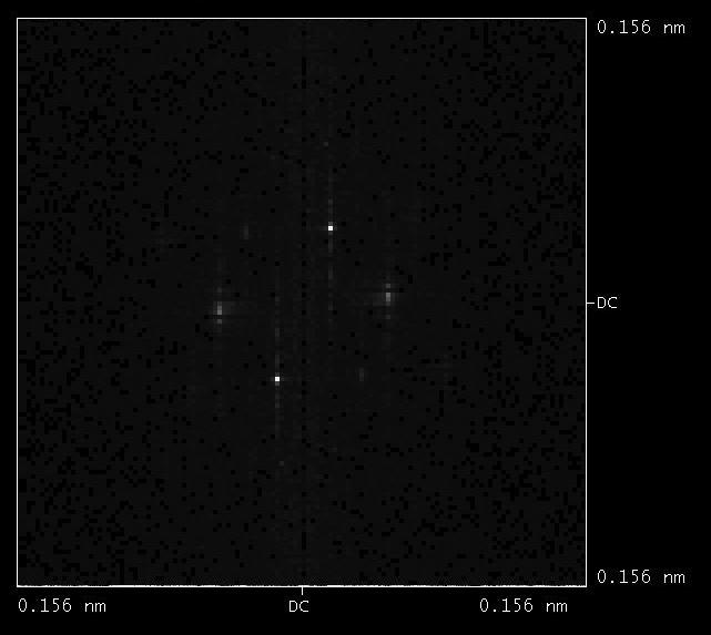 While periodic structures are clearly visible, they are barely resolvable through noise-- though some parts of the frame are better than others. The periodic nature of the image and aperiodic nature of the noise allows one to use spectral filtering to remove the noise and restore the image. The second image in this example shows a 2D FFT of the image showing spatial frequencies in a hexagonal pattern representing the signal from the mica surface mesh. Pass bands can be placed around these regions allowing one to reconstruct the image solely with the spectral information presumed to be from the mica surface mesh. This is a more robust method of processing an image of a periodic structure than low pass or median filtering.
 The 3D image is the frame above reconstructed by placing pass bands on the six-fold symmetric bands in the 2D-FFT shown above. A nice hexagonal surface net is clearly visible. The surface net of muscovite mica has a lattice parameter of 0.52 nm. The measured lattice parameter is about 0.58 nm and varies slightly depending upon the part of the frame used to estimate the lattice parameter. There is also a slight difference in the lattice parameter (~ 8%) depending upon which high symmetry direction is used for the measurement.
The best way to measure the lattice parameter is to use the spectral content of the entire image. There is a great potential for error in taking sections from data with this amount of noise, whether the data is filtered using pass-bands in the 2D FFT or not. The final image shows the 2D power spectrum which shows the dominant frequency at 0.528 nm-- very close to the muscovite lattice parameter.
 UHV SPM's used routinely for atomic imaging allow one to heat clean and reconstruct a surface prior to imaging. Even in such systems mica images are less clear than the classic Si(7x7) reconstruction. Systems like the Dimension 3000 are seldom calibrated using atomic scale standards because of the difficulty in obtaining high quality images through the various forms of noise inherent in the system. As such the miscalibration and astigmatism of these atomic level images is not considered unusual.
The purpose of this example is to show that atomic level images are possible with the Dimension 3000, and to point out some of the concerns in obtaining such images as they apply to other high resolution imaging problems.


