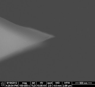
 The probe radius is the primary design parameter related to resolution. The process of tip qualification to measure the probe radius using a sample with sharp features has been discussed in a previous blog entry. An effective probe radius can be also be measured using controlled deformations while measuring the modulus of a material with known modulus. These methods of measuring probe radius are required for mechanical measurements as well as certifying image quality.
 The degradation of the probe radius will impact image resolution as the surface features are convoluted with a larger than anticipated probe radius. A "sharp" probe might have a radius of 3-5 nm, so a blunting to 30-50 nm will result in the dramatic loss of image quality. Probes coated with conducting material, such as platinum or aluminum, will have additional artifacts in such modes as TUNA or conductive AFM in the current channels due to the loss of conducting contact area with the sample.
 In this post visible apex AFM probes were imaged in a field emission SEM. This probe, the Bruker OTESPA, is called a visible apex probe because the functional part of the probe is at the very end of the cantilever, allowing one of locate objects of interest in the optical microscope of the AFM very easily. The probes were imaged with a 2 kV beam using the through lens detector and field immersion. The larger top image shows a good probe. Even at 2 kV parts of the probe appear to be "transparent" as SE1 secondary electrons are generated near the edges of the probe, while SE2 secondary electrons are generated from the thicker body of the probe.
It is common for probes to fail not only by being blunted or worn-- from their radius being drastically increased-- but from picking up objects. The smaller images show three examples of failed OTESPA probes. The probes showed lower resolution and in all cases either self-similar structures or features with companions. These SEM images show objects attached to the probe. In the second image a blunt object is stuck near the end of the probe, and the shape of this object where it contacts the surface would be convoluted with the sample features. In the third image a sharp object is attached just behind the probe. This can act as an companion probe that contacts features and probes companions or doubles to sample features. The last image shows deposition of material across much of the probe, and the attachment of a significantly large foreign object. An object of this size will not only degrade image quality by make the probe very unstable as it interacts with the surface.
The point of this post is to show that things really do go wrong with a probe when image quality degrades.


